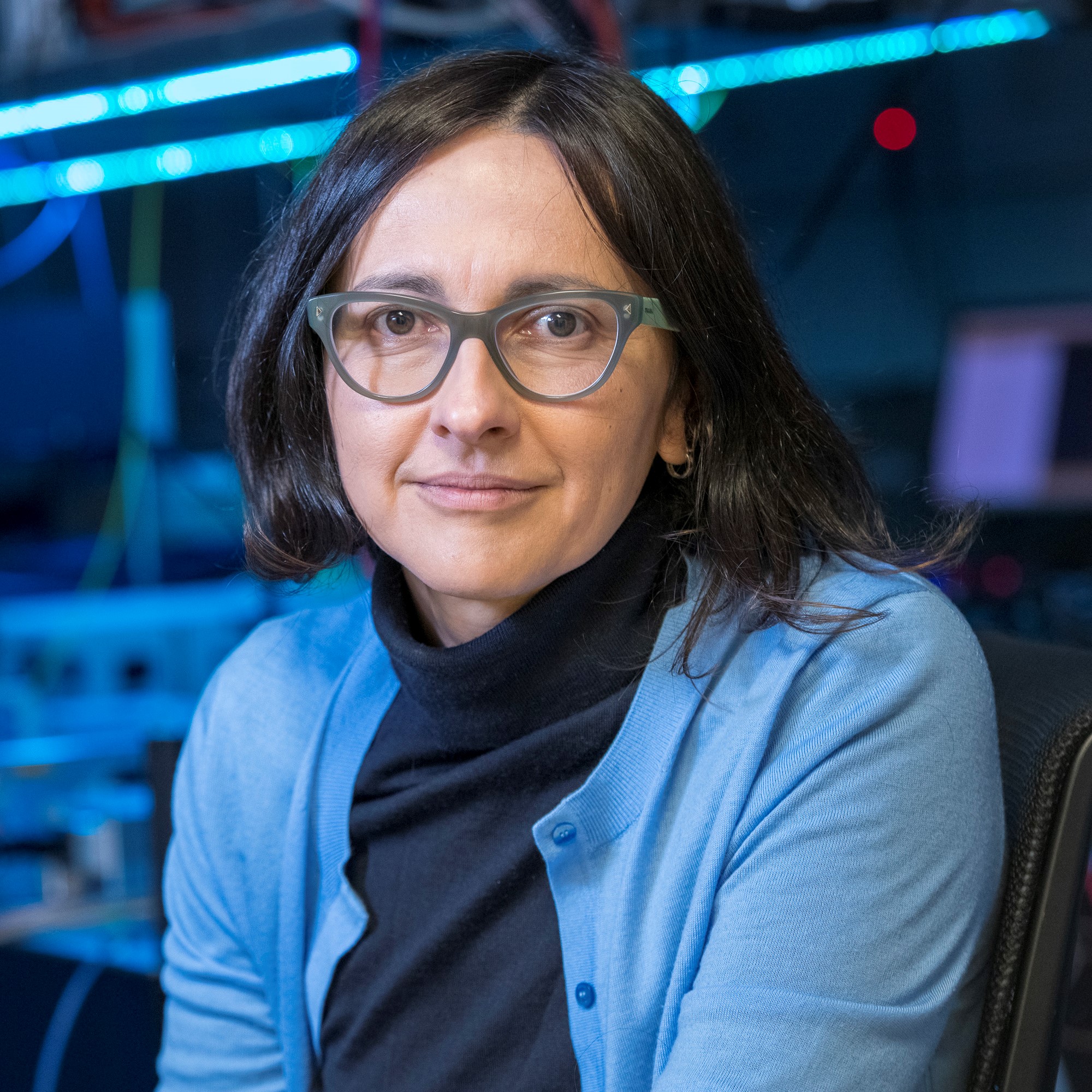
Jelena Vuckovic, Stanford University
(Approved for Public Release)
Quantum entanglement provides a key resource for all quantum technologies, ranging from quantum computing and quantum error correction to secure quantum communication and quantum metrology. These technologies are of great relevance to the DoD, as they could eventually provide platforms for unconditionally secure long distance information transfer, for solving problems currently unsolvable with the most powerful computers, or for compact and portable sensors with superior properties relative to the state of the art.
However, central challenges remain in the engineering, manipulation, and application of large-scale entanglement. Record sizes of maximally entangled qubit systems are still quite modest in all platforms, with at most 24 qubits entangled in a GHZ state. On the other hand, the largest quantum network consists of only 3 remotely entangled nodes.
The key goal of this proposal is to address this central challenge of quantum science and engineering by developing a new semiconductor platform for producing and manipulating large entangled states of light and matter. This is disruptive to the current research directions of quantum information science, and relies on engineered materials, novel optimization tools, and new experimental techniques. The fundamental science questions that this work aims to address are the studies of light - matter interaction and cavity quantum electrodynamics on scales that have previously not been accessible, the size limits of maximally entangled states, but also whether semiconductors could be used to build large scale quantum systems.
We present a vision of how a platform consisting of a wafer-scale semiconductor - silicon carbide, with quantum photonics devices which are incorporating positioned and tunable color centers (crystal defects with optical transitions that enable spin-to-photon interfaces) can be used to implement massive entangled states, as well as a scalable, modular, fault tolerant quantum computing architecture. Color centers acting as spin qubits are interfaced and controlled by optical and microwave fields, and are electrically tunable, allowing for the compensation of spectral broadening and in homogeneities resulting from the nonuniform solid state environment. Interactions between qubits are optically mediated via tuning into many available cavity modes for entanglement.
We show how qubit coherence can be surprisingly preserved in these CMOS-compatible fabricated structures that are necessary for their efficient interfacing. High fidelity single and two-qubit gates can also be implemented and fully parallelized. In this architecture, nuclear spin registers in the host crystal proximal to electron qubits are used as a quantum memory, and for fault tolerant encoding of logical qubits.
We believe that silicon carbide is an ideal material for answering the key goals of the proposed research and for completely changing the landscape of quantum science and engineering - essentially what silicon did for classing computing. This material hosts high quality qubits that can be entangled, interfaced, and processed in a parallelized and fault tolerant way using optical photons, while also displaying a set of properties not available in any other platform. These include monolithic electronic and photonic circuits, full silicon CMOS processing compatibility, strong optical nonlinearities for frequency conversion and electro-optic switching, piezoelectricity, superb micro-mechanical and thermal properties, and the opportunity to incorporate qubits with atomic precision. All of these combined features offer a unique way to address all challenges in scaling of quantum systems, including the inhomogeneity and imperfections of qubits, the inability to precisely control