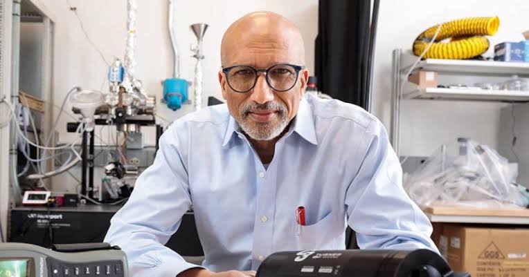
Supratik Guha / The University of Chicago
Atomic imprint crystallization and scanning near-field deposition for creating large area single crystal surfaces on amorphous substrates
(Approved for public release)
Project Narrative – Statement of Objectives
Our proposed project asks the question: is it possible to create large area thin single crystal semiconductor layers on amorphous substrates in a scalable fashion? Our objective is to demonstrate this by carrying out the underlying materials science and developing two as yet unexplored experimental vehicles: (i), crystallization via the control of a seeding periodic potential whose strength and distance can be varied; and (ii), the kinetics of nanoscale epitaxy for creating thin (few monolayers) epitaxial layers using near-field scanning probe vapor deposition at <50 nm lateral resolution. In (i) we will carry out the science and build the experimental equipment needed to bring a single crystal atomic surface in contact with an amorphous semiconductor surface, use the periodic potential on the single crystal surface to initiate epitaxial crystallization in the amorphous layer, and then debond and retract the crystalline surface non-destructively. This requires an understanding of the interplay between the interatomic potentials for initiating crystallization, and the fracture process for cleaving the crystallized interface. It requires us to understand how to control the strength of the interaction between a crystalline surface and an amorphous layer by introducing interleaving amorphous monolayers or physisorbed/chemisorbed layers so that crystallization and fracture processes may be exquisitely controlled. For this we will develop first principles physics models informed by machine learning for molecular dynamics simulations of the epitaxial crystallization process and the debonding/fracture process: results from these simulations will feed into the experiments. In (ii) we will rethink epitaxy at the nanoscale by building and using near field chemical vapor deposition capabilities using nanoscale nozzles and slits (<50 nm) mounted on scanning probe stages. This involves understanding epitaxy of very thin single crystal surface layers where the epitaxial growth front is drawn laterally by the scanning probe deposition equipment with <50 nm lateral deposition resolution from starting epitaxial seeds. This is a new approach, unlike most other treatments of epitaxy, which employ a broad beam source that impinges on the surface from the far-field. We will accomplish this via demanding experimental efforts in controlling the materials, thermal and scanning processes, and modeling of the multi-physics processes involved—thermal effects, phase transformations, surface chemistry, diffusion and vapor phase crystal growth. Following successful demonstration of (i) using Si-Ge as a model system, we will extend the research to demonstrating the deliberate placement of native point, dopant and line defects at predetermined sites by exploiting the lateral resolution of the probes. We will also explore the potential for “writing” additive epitaxial three dimensional structures using this technique for novel device architectures of the future.
If our project is successful, we will develop the science that will allow us to create large, scalable single crystal semiconductor surfaces on arbitrary substrates. Amorphous layers would be crystallized by imprinting with a crystalline stamp, followed by retraction of the stamp. This has not been achieved before and it would offer unprecedented degrees of freedom to photovoltaic and microelectronics technologies. We would have developed and understood near field scanning probe epitaxy, with lateral epitaxial resolution of <50 nm. We would have developed and understood the underlying materials science for creating single crystal surfaces of semiconductors at will and on arbitrary substrates.